This article will be a little different from most on the PIRL site because it’s written about a non-coder that happens to look at persistent memory as a business more than as a technology. It relates to the readers, though, since we try to project where this technology is headed and how it should impact programming and the development of new approaches to coding to take the best advantage of the new technologies.
This is based upon a report we wrote called “Emerging Memories Ramp Up”: (https://Objective-Analysis.com/reports/#Emerging) that explores the market for these technologies and the tools used to produce them. If you know anyone who could use this report we would love your telling them about it.
All Those Memory Types
Emerging memories have been around for decades. In fact, one of the earliest emerging memory chips was a 256-bit phase-change memory (PCM or PRAM) prototype designed by a team led by Gordon Moore of Moore’s Law fame. This was described in the cover article for the 28 September 1970 issue of Electronics Magazine, a copy of which can be found here: https://Objective-Analysis.com/fun-stuff/. PCM is the basis for the Intel/Micron 3D XPoint Memory which Intel merchandises using the Optane brand name.
(The article’s lead author, Ron Neale, still writes posts about PCM for The Memory Guy blog at https://TheMemoryGuy.com.)
Over time several other technologies evolved, including Magnetic RAM (MRAM), Resistive RAM (ReRAM), Ferroelectric RAM (FRAM), and many others. Each of these employs a technology that differs from today’s standard memory technologies (DRAM, NAND flash, NOR flash, SRAM, and EEPROM) because it is not charge-based, that is, the difference between a 1 and a 0 depends on the number of electrons stored in a memory bit cell. The new memories store bits with other mechanisms including magnetism, variable resistance, the position of an atom within a crystal, etc. With the exception of certain forms of ReRAM these technologies also use new materials that are not commonly found in semiconductor processing.
Another very important difference between these technologies and today’s leading memory types is that they are nonvolatile (unlike DRAM and SRAM) and can be overwritten, without being pre-erased, with write latencies that are similar to their read latencies (unlike NAND, NOR, and EEPROM). They promise to vastly simplify the ideal of bringing storage close to the processor.
But that’s not the reason that they have received a steady flow of research funding since the 1960s. The single most desirable property of these technologies is that they promise to reach lower price points than can today’s technologies.
The Scaling Limit
The semiconductor industry embodies Moore’s Law by shrinking transistors – producers have continually increased the number of transistors “printed” onto a chip by shrinking their length and width, an approach commonly called “Scaling”. This is how chip makers have followed the path first observed by Moore in 1965, in which the number of transistors on a chip doubled every year or two, leading to a commensurate decrease in the cost per gigabyte of memory.
For nearly the entire lifetime of the chip market manufacturers have worried that eventually this approach would come to an end. Although many have projected the “Scaling Limit” of various semiconductors, and although these projections have led to several premature announcements of the death of Moore’s Law, the back-room geniuses at semiconductor manufacturers have repeatedly been able to devise amazingly creative ways to push scaling a few more process nodes ahead to bring us where we are today.
What would happen to memories if a scaling limit actually did occur? The conceptual chart below explains that.
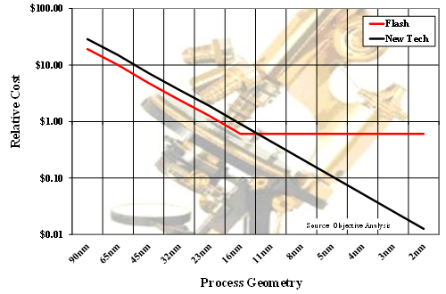
In this figure the horizontal axis represents the memory chip’s smallest printed feature which, over time, has moved from hundreds of microns (millionths of a meter) down to today’s 1Z nanometer (billionths of a meter) process. Future processes are expected to shrink even smaller. (Note that in this chart the larger processes are on the left and the smaller ones on the right to make the chart follow the progress of time. Vertical lines represent a time interval of about two years.)
The vertical axis gives a relative cost per gigabyte for the memories in the chart. It is plotted logarithmically for two reasons:
- With a linear scale the red and black lines would be nearly vertical at the left side of the chart, then would hug the bottom axis for the remainder of the chart. It would therefore be impossible to discern a difference between the red and the black line on the right half of the chart.
- In this sort of semilogarithmic chart constant growth appears as a straight line. The straight decline of both lines is about 30% per year, which corresponds to Moore’s Law.
The red line gives us the relative production cost per gigabyte of standard flash memory. As the process geometry scales, the cost decreases until the scaling limit is reached and the red line stops its descent.
The black line represents an emerging technology (“New Tech”) whose wafer cost has been arbitrarily set 50% higher than that of flash. In this model all else is the same between the emerging memory and the flash, including the number of bits per square millimeter, so the emerging memory will always cost 50% more to make than flash. Since this hypothetical technology can scale past flash’s scaling limit, the new technology simply needs to scale to the next process geometry after flash’s scaling limit to beat flash’s cost structure, even though the new technology’s wafer cost is higher than flash. This is the reason why investors and corporations continue to invest in emerging memory technology R&D.
(I should note that NAND flash reached its scaling limit at 15nm and further process shrinks would be unable to produce smaller cells. Emerging memories were positioned to take over the NAND market after the 15nm node, but NAND researchers devised the 3D NAND process, and that allowed them to continue to increase the number of transistors on a chip even without further process shrinks. Without the development of this 3D approach NAND’s cost would have leveled off, as is shown with the red line.)
All of those new memory technologies have been developed with this in mind – they promise to continue to scale once established memory technologies reach their scaling limits.
Where We Are Today
Since NAND flash found a way past its scaling limit where does that leave emerging memories?
None of the other established technologies is in trouble. NOR flash, SRAM, and EEPROM aren’t used in applications that are as sensitive to the cost of a large memory array as are DRAM and NAND flash applications, so they aren’t produced on processes that are even close to reaching their scaling limits. DRAM still has a number of years ahead with new shrinks that should support the technology for another decade or so.
That means that these new memory technologies would normally be relegated to niche markets where their higher cost could be justified by their technical benefits. MRAM and FRAM are the only two that have been produced in high volume, with MRAM winning designs that normally would have used an SRAM plus a backup battery and with FRAM going into RFID cards in which the power to write to the FRAM comes solely from the interrogating radio waves. Both of these technologies have found a way into journaling applications in certain storage devices (as in an IBM FlashCore module SSD released in 2018), but such sightings are very unusual and are often short-lived.
The only emerging memory that is currently being aimed at computing markets is the Micron/Intel 3D XPoint Memory. This memory is a key part of Intel’s Cascade Lake platform which requires the new technology to strikingly outperform prior generations.
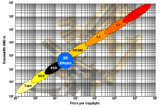
The 3D XPoint memory, which Intel provides under the “Optane” brand, is intended to sell into the memory/storage hierarchy to fit between NAND flash SSDs and DRAM: It is faster than NAND flash, yet slower than DRAM, and must be priced less than DRAM although it can be priced higher than NAND flash. It then fits into the memory/storage hierarchy as is illustrated in the figure below.
This approach doesn’t try to capitalize on XPoint’s persistence, since software that harnesses this attribute is not yet widely available. The technology must win its place in the market when used as a cheaper alternative to expanding DRAM.
This is a good approach, not only because of the lack of software, but also because Intel and Micron need to manufacture an enormous volume of this chip to get its production cost in line with the required selling price. This has proven challenging for the companies to date, and Intel has plowed billions of dollars into the program which has lost money since its introduction.
What the Future Holds
Coders probably want to know what the outlook is for the future, and what skills they will need to be at the forefront of this technology. We will continue to look at this from the perspective of memory technologies to tell where we see the market going.
First of all, we need to divide the market into two components: 3D XPoint/Optane and everything else. This is because Intel’s sponsorship of 3D XPoint provides that technology with an advantage that is unavailable to other memories that will limit overlap between the two.
The non-XPoint segment will continue to struggle with its cost disadvantage compared against today’s established technologies. The chart below, taken from our emerging memories report illustrates how an emerging memory technology will take advantage of its smaller bit size to drive its cost below SRAM and NOR flash prices in the near term, and eventually fall below DRAM as it approaches NAND-like costs. For simplicity’s sake we labeled the line “MRAM”, but it could be any of the other new technologies: The race hasn’t been decided yet, and any of them could pull ahead of the others.
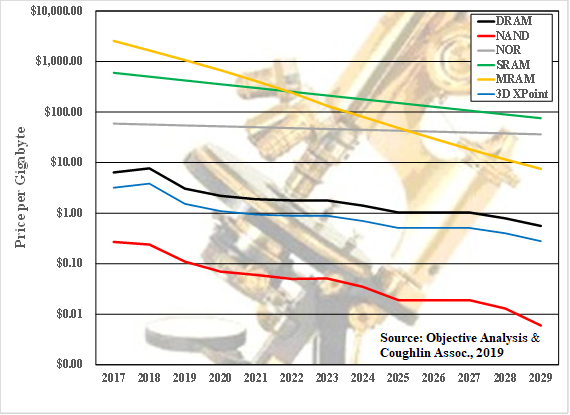
As the MRAM line falls below the lines for other technologies hardware designers will choose the new technology rather than the older one simply to take advantage of its price benefit. Programmers will then be given new options to use a fast-write nonvolatile technology where they once had been put under greater constraints, and this can be tapped to add new features to a system.
Forward-thinking programmers who see a way to harness these technologies may be able to convince management to let them influence the hardware designer’s choice a bit – if a compelling feature can be added perhaps the design team can justify using a more costly memory technology. These battles, though, will be hard won.
Extend this chart past 2029 and it appears likely that the new memory could cross DRAM’s price to replace the memory in most systems. This will be especially true since DRAM’s average annual manufacturing cost decline is expected to slow, and that will make this chart resemble the first chart in this post. We anticipate, though, that the new technology’s price decline will start to ease before it reaches the cost of 3D XPoint Memory. Most of these new memories will share a cost structure very similar to that of 3D XPoint memory once both products are in very high-volume production.
As for 3D XPoint technology: if we assume that Intel continues to subsidize the technology until it becomes profitable (which appears very likely) it will continue to be priced below DRAM, allowing its market to grow by taking away a share of the IT industry’s DRAM spend.
The fact that the system administrator can choose between a large fast DRAM or a much larger, somewhat slower combination of DRAM and 3D XPoint memory we see that many applications will be able to move into a much larger memory space without any change to the application software. Intel has named this “Memory Mode” and it is described in some detail HERE.
More important to the programmer, though, is App Direct Mode, described HERE, in which the 3D XPoint Memory is found in its own address range which can be used as persistent memory to avoid slow storage I/O when data needs to be persisted. The techniques for harnessing this have been standardized via the SNIA Non-Volatile Memory Programming Model, which has already been embodied in Linux, Windows, and other operating systems. In about a decade some programmers will find it amazing that the world could have existed without persistent memory.
Already certain applications have been adapted to persistent memory. The most notable ones are databases, particularly the proprietary ones used by hyperscale Internet data centers, but eventually there will be a large base of standard commercial software that can use persistence to accelerate performance.
In a nutshell, persistent memory is upon us, in the form of emerging memory technology. Programmers who wish to remain competitive should take the time to understand SNIA’s work and investigate ways to use persistence to their advantage.
Jim Handy of Objective Analysis has over 35 years in the electronics industry including 20 years as a leading semiconductor and SSD industry analyst. Early in his career he held marketing and design positions at leading semiconductor suppliers including Intel, National Semiconductor, and Infineon. A frequent presenter at trade shows, Mr. Handy is known for his technical depth, accurate forecasts, widespread industry presence and volume of publication. He has written hundreds of market reports, articles for trade journals, and white papers, and is frequently interviewed and quoted in the electronics trade press and other media. He posts blogs at www.TheMemoryGuy.com, and www.TheSSDguy.com.

This work by Jim Handy. is licensed under a Creative Commons Attribution-NonCommercial-NoDerivs 4.0 International